Spin and Charge Based Quantum Devices
Some of the best fundamental science of the modern era (the quantum Hall effect, fractional quantum Hall effect, single electron transistors, electron spin based qubits), and some of the most technologically significant device developments (HEMTs, pHEMTs) have relied on many years of investment in III-V semiconductor heterostructure two dimensional electron gases (2DEGs) and the development of associated sophisticated field effect devices using these electron or hole conducting layers.
Whilst numerous materials systems have been exploited in a wide number of applications and markets, the most extreme heterostructure variant based around Indium Antimonide (InSb/InAlSb) has received less attention due to the considerable technological difficulties presented in mismatched epitaxial growth and general immaturity of device processing and handling.
However, InSb has the highest electron mobility, smallest electron effective mass, longest mean free path, and longest ballistic length of all the III-V semiconductors. It also has an extremely large spin-orbit interaction and associated high Lande g-factor (up to ~-60 [ref] compared to ~-0.6 for GaAs based materials). The benefits of working on semiconductor heterostructures using this challenging material are considerable.
Detail
All electrical control of single electron spins would be a major breakthrough. This work aims to demonstrate single electron manipulation in multi-gate field effect structures, and demonstrate the potential for spin manipulation using the Rashba effect for spin splitting of the quantised 2DEG electron states. High temperature operation will also be explored, resulting in easier and cheaper experimental measurement environments compared to other similar solid state qubit solutions.
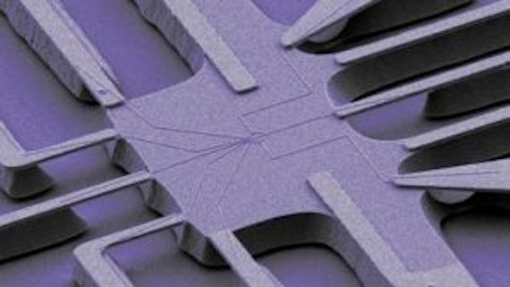
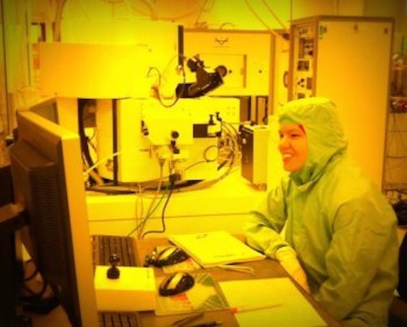
The work builds on basic building block devices (split gate structures, single electron transistors) that have been published previously, and uses specialist tailored processing in the Cardiff cleanroom, including high resolution electron beam lithography (pictured). Devices are assessed in a newly established low temperature novel device measurement capability. Material is being grown by our close collaborators at the National Centre for III-V technologies at the University of Sheffield.
Previously this technology was a world lead for the UK at QinetiQ/DERA Malvern. Moving this technology forward for wider exploitation within the UK scientific community is a high priority for this work. Exploiting the novel properties will lead to a rich vein of fundamental quantum device study.
Publications
- Gilbertson, A. M. et al., 2011. Room temperature ballistic transport in InSb quantum well nanodevices. Applied Physics Letters 99 (24) 242101. (10.1063/1.3668107)
- Gilbertson, A. M. et al., 2011. Suppression of the parasitic buffer layer conductance in InSb/AlxIn1-xSb heterostructures using a wide-band-gap barrier layer. Physical Review B 84 (7) 75474. (10.1103/PhysRevB.84.075474)
- Gilbertson, A. M. et al., 2009. Zero-field spin splitting and spin-dependent broadening in high-mobility InSb/In1-xAlxSb asymmetric quantum well heterostructures. Physical Review B 79 (23) 235333. (10.1103/PhysRevB.79.235333)
- Orr, J. M. S. et al., 2007. A surface-gated InSb quantum well single electron transistor. New Journal of Physics 9 (8) 261. (10.1088/1367-2630/9/8/261)