Newport Wafer Fab Ltd
Academics from our Institute for Compound Semiconductors delivered a short course 10 times to 80 staff at Newport Wafer Fab Ltd.
The training allowed staff from across the organisation to enhance their knowledge of compound semiconductor electronics and photonics production.
Newport Wafer Fab excels in the fabrication of silicon wafers (ie a semiconductor) and is also a development centre for compound semiconductors and photonics production. This training was commissioned to provide their employees with an overview of compound semiconductor electronics and photonics, so that they have an increased understanding of how these technologies could be integrated successfully with the organisation’s existing procedures.
Creating a bespoke training programme
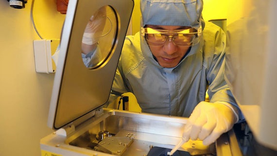
In the months before the training, academics from the ERDF-funded Institute for Compound Semiconductors visited the company’s 'Fab' (a Class 1 cleanroom environment) and met with managers of various departments to understand their day-to-day roles and their requirements for the course. Our staff from the Continuing Professional Development (CPD) Unit helped facilitate this as we have established relationships with University academics and teaching staff.
We also provided project management and administrative support.
Course content
This one-day course consisted of three main sessions.
Session one
An overview of Newport Wafer Fab’s existing expertise and current production procedures, delivered by one of the company’s senior engineers.
Session two
An introduction to compound semiconductor electronics production, delivered by a senior academic from Cardiff School of Engineering. The session covered:
- The definition of a compound semiconductor
- How compound semiconductors differ from silicon (i.e. a semiconductor material)
- The different types of compound semiconductor materials available, their benefits, their properties and how they each perform in electronic integrated circuits
- The uses of different compound semiconductor materials in the marketplace
- The opportunities, challenges and risks that introducing compound semiconductor materials present to Newport Wafer Fab and their existing electronics production processes
Session three
An introduction to photonics production, delivered by an experienced lecturer at Cardiff School of Physics and Astronomy. This session covered the following:
- What is silicon photonics?
- What are the current marketplace applications and future opportunities for silicon photonics?
- Why use silicon as a photonics material and what are its advantages and disadvantages?
- Understanding passives versus actives in the silicon photonics process
- What are the building blocks of silicon photonics, including: waveguides, grating couplers, resonators, filters, and switches and modulators?
Thank you to Cardiff University for a fantastic delivery. Those who have attended have told me that this is one of the best technical courses they have been on. The pitch and pace is good and the delivery is relaxed. Staff feel comfortable to ask questions and to enjoy the day.
About Newport Wafer Fab Ltd
Newport Wafer Fab Ltd is the UK’s largest semiconductor centre, making approximately 8,000 wafers a week. Its foundation is in silicon; taking silicon wafers and developing them into wafer products for a variety of sectors such as the automotive, medical, industrial and consumer industries. They are experts in power MOSFET products, widely used in switching applications. Newport Wafer Fab is also the world’s first eight inch compound semiconductor on silicon chip foundry and is a development centre for compound on silicon and for photonics. It’s a member of CS Connected, the world’s first compound semiconductor cluster.
About the Institute for Compound Semiconductors (ICS)
The ICS is a pay to use Open Access Fabrication Facility, targeted at translational Compound Semiconductor research. It has associated academics in both Cardiff School of Engineering and Cardiff School of Physics and Astronomy concentrating on Compound Semiconductor material and device research. As part of the CS Cluster its aim is to create a global hub for Compound Semiconductor technology research, development and innovation.
The Institute is currently involved in research around developing next-generation technology that paves the way for 5G and 6G mobile phone networks, photonic integrated circuits for applications in e.g. data communications and lidar, the use of sensors in healthcare and energy applications, and the development of advanced radar systems (amongst other uses). It is a core partner in CS Connected. The Institute will be housed in a new state-of-the-art centre that will form part of Cardiff University's Innovation Campus.
Investment in people’s skills is essential to the growth of the compound semiconductor sector here in South Wales. Cardiff University is delighted to be working with Newport Wafer Fab on a number of levels and I hope this is the start of a long and fruitful partnership.
Other collaborations between the University and Newport Wafer Fab Ltd
This short course has led to other collaborative activities between the two organisations. Newport Wafer Fab agreed to fund three PhD students for the 2019-20 academic year. It is providing ongoing support to the University with regard to training opportunities for MSc and PhD students, and in the University’s recent successful bid for a new EPSRC funded Centre for Doctoral Training (CDT) in Compound Semiconductor Manufacturing.
Newport Wafer Fab is working with Cardiff School of Engineering and Cardiff School of Physics and Astronomy to offer final year students work placement activities and tours of their Fab. The company also plans to work with Cardiff Business School, who will develop and deliver a new leadership programme for their senior staff.
Contact us
If you would like to discuss bespoke training opportunities for your organisation, please contact our friendly team. We act as a gateway for businesses to connect with academic expertise across the University, and can work with you to create a programme that works for you.
Continuing Professional Development Unit
We offer a gateway for businesses to access the wide range of expertise available within Cardiff University.
